- 您现在的位置:买卖IC网 > Sheet目录3832 > PIC16F876A-I/SP (Microchip Technology)IC MCU FLASH 8KX14 EE 28DIP
2003 Microchip Technology Inc.
DS39582B-page 129
PIC16F87XA
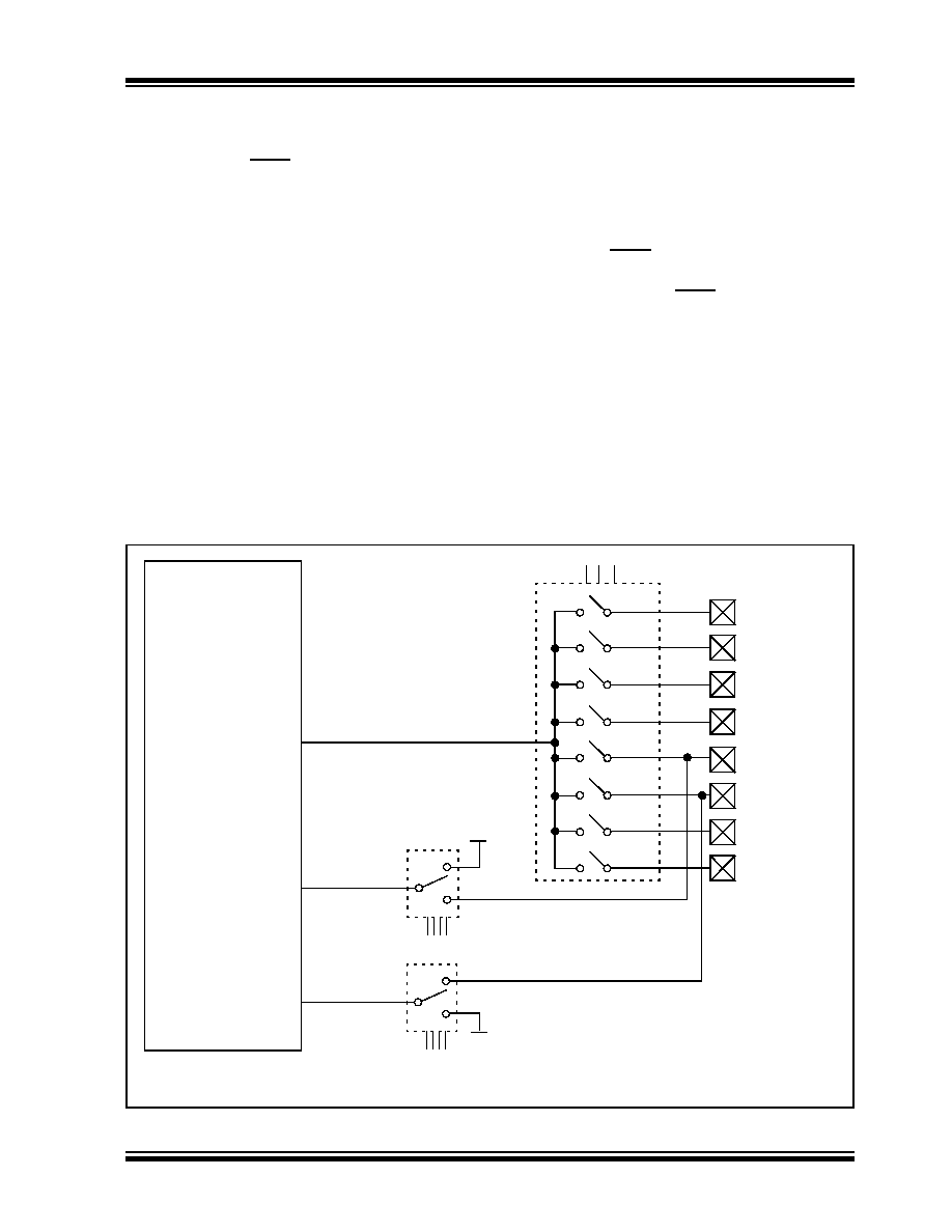
The ADRESH:ADRESL registers contain the 10-bit
result of the A/D conversion. When the A/D conversion
is complete, the result is loaded into this A/D Result
register pair, the GO/DONE bit (ADCON0<2>) is cleared
and the A/D interrupt flag bit ADIF is set. The block
diagram of the A/D module is shown in Figure 11-1.
After the A/D module has been configured as desired,
the selected channel must be acquired before the con-
version is started. The analog input channels must
have their corresponding TRIS bits selected as inputs.
To determine sample time, see Section 11.1 “A/D
Acquisition Requirements”. After this acquisition
time has elapsed, the A/D conversion can be started.
To do an A/D Conversion, follow these steps:
1.
Configure the A/D module:
Configure analog pins/voltage reference and
digital I/O (ADCON1)
Select A/D input channel (ADCON0)
Select A/D conversion clock (ADCON0)
Turn on A/D module (ADCON0)
2.
Configure A/D interrupt (if desired):
Clear ADIF bit
Set ADIE bit
Set PEIE bit
Set GIE bit
3.
Wait the required acquisition time.
4.
Start conversion:
Set GO/DONE bit (ADCON0)
5.
Wait for A/D conversion to complete by either:
Polling for the GO/DONE bit to be cleared
(interrupts disabled); OR
Waiting for the A/D interrupt
6.
Read
A/D
Result
register
pair
(ADRESH:ADRESL), clear bit ADIF if required.
7.
For the next conversion, go to step 1 or step 2
as required. The A/D conversion time per bit is
defined as TAD.
FIGURE 11-1:
A/D BLOCK DIAGRAM
(Input Voltage)
VAIN
VREF+
(Reference
Voltage)
VDD
PCFG3:PCFG0
CHS2:CHS0
RE2/AN7(1)
RE1/AN6(1)
RE0/AN5(1)
RA5/AN4
RA3/AN3/VREF+
RA2/AN2/VREF-
RA1/AN1
RA0/AN0
111
110
101
100
011
010
001
000
A/D
Converter
Note
1: Not available on 28-pin devices.
VREF-
(Reference
Voltage)
VSS
PCFG3:PCFG0
发布紧急采购,3分钟左右您将得到回复。
相关PDF资料
AT87C51RD2-3CSUM
IC 8051 MCU 64K OTP 40MHZ 40DIP
DSPIC33FJ64MC802-I/SO
IC DSPIC MCU/DSP 64K 28-SOIC
DSPIC33FJ64GP802-I/MM
IC DSPIC MCU/DSP 64K 28-QFN
AT87C51RD2-3CSUL
IC 8051 MCU 64K OTP 30MHZ 40DIP
PIC18F2431-I/SP
IC PIC MCU FLASH 8KX16 28DIP
AT87C51RC2-SLSUM
IC 8051 MCU 32K OTP 40MHZ 44PLCC
PIC18F2520-I/ML
IC PIC MCU FLASH 16KX16 28QFN
AT87C51RC2-SLSUL
IC 8051 MCU 32K OTP 30MHZ 44PLCC
相关代理商/技术参数
PIC16F876A-I/SP
制造商:Microchip Technology Inc 功能描述:IC 8BIT FLASH MCU 16F876 SDIL28
PIC16F876A-I/SPG
功能描述:8位微控制器 -MCU 14KB 368 RAM 22 I/O RoHS:否 制造商:Silicon Labs 核心:8051 处理器系列:C8051F39x 数据总线宽度:8 bit 最大时钟频率:50 MHz 程序存储器大小:16 KB 数据 RAM 大小:1 KB 片上 ADC:Yes 工作电源电压:1.8 V to 3.6 V 工作温度范围:- 40 C to + 105 C 封装 / 箱体:QFN-20 安装风格:SMD/SMT
PIC16F876A-I/SS
功能描述:8位微控制器 -MCU 14KB 368 RAM 22 I/O RoHS:否 制造商:Silicon Labs 核心:8051 处理器系列:C8051F39x 数据总线宽度:8 bit 最大时钟频率:50 MHz 程序存储器大小:16 KB 数据 RAM 大小:1 KB 片上 ADC:Yes 工作电源电压:1.8 V to 3.6 V 工作温度范围:- 40 C to + 105 C 封装 / 箱体:QFN-20 安装风格:SMD/SMT
PIC16F876A-I/SS
制造商:Microchip Technology Inc 功能描述:8BIT FLASH MCU SMD 16F876 SSOP28
PIC16F876A-I/SSG
功能描述:8位微控制器 -MCU 14KB 368 RAM 22 I/O RoHS:否 制造商:Silicon Labs 核心:8051 处理器系列:C8051F39x 数据总线宽度:8 bit 最大时钟频率:50 MHz 程序存储器大小:16 KB 数据 RAM 大小:1 KB 片上 ADC:Yes 工作电源电压:1.8 V to 3.6 V 工作温度范围:- 40 C to + 105 C 封装 / 箱体:QFN-20 安装风格:SMD/SMT
PIC16F876AISP
制造商:Microchip Technology Inc 功能描述:
PIC16F876AISS
制造商:MICROCHIP 功能描述:IC, MICRO CONTROLLER SSOP28
PIC16F876AT-E/ML
功能描述:8位微控制器 -MCU 20MHz 8K Flash RoHS:否 制造商:Silicon Labs 核心:8051 处理器系列:C8051F39x 数据总线宽度:8 bit 最大时钟频率:50 MHz 程序存储器大小:16 KB 数据 RAM 大小:1 KB 片上 ADC:Yes 工作电源电压:1.8 V to 3.6 V 工作温度范围:- 40 C to + 105 C 封装 / 箱体:QFN-20 安装风格:SMD/SMT